
By Shawn Back, ON Semiconductor.
The KNX standard provides users or BUS installers the benefit of interoperability among a number of KNX device manufacturers. In order to ensure successful communication between devices, a strict certification process established by the KNX organisation is required for both the hardware and software.
When developing a new KNX device, the engineering work is easier if the hardware and software are pre-certified compared to designing the electronic circuits and programming the corresponding KNX stack from scratch. This guidance also applies when diversifying products with a variety of platform designs.

KNX transceiver design options
When designing a KNX transceiver module, there are several options available:
1) Buying a commercialised transceiver PCB module.
2) Integrating an off-the-shelf transceiver IC and microcontroller on a separate printed circuit board for KNX communication.
3) Designing a complete application with a KNX transceiver and versatile microcontroller on a single board
The first is the fastest way to design a KNX device thanks to the pre-certification of the KNX transceiver module. This results in a reduced set of tests for certification of the complete application, simplifies the hardware and software integration and ultimately the registration of the device through the KNX Association. This is an excellent option for companies who have recently joined the KNX organisation, are new to building KNX devices and would like to release a product to market quickly.
Option 2 is the most common method of developing a KNX device as it provides greater design flexibility when selecting the transceiver, microcontroller, KNX stack and the PCB layout. This also allows the platform to be integrated into various applications. In this implementation, having a certified KNX platform makes it is easy to proliferate KNX devices by application. High-volume manufacturers who build a rich portfolio of KNX devices typically follow this option.
Option 3 requires a skilled designer to integrate everything into a single board. This method provides a number of benefits including a smaller system size and less expensive BoM (Bill of Materials) cost, but will also require a full certification test. High-volume production of the device can compensate for the extra effort and cost required.
For Options 2 and 3, there are typically fewer certified transceivers available compared to other electronic components.
Pre-certified KNX transceivers
ON Semiconductor offers a complete portfolio of pre-certified KNX transceivers designed specifically for different application needs. These products were developed with the same design architecture and package (40-pin 6×6 QFN), allowing manufacturers to replace ICs with a simple change of PCB layout and external components.
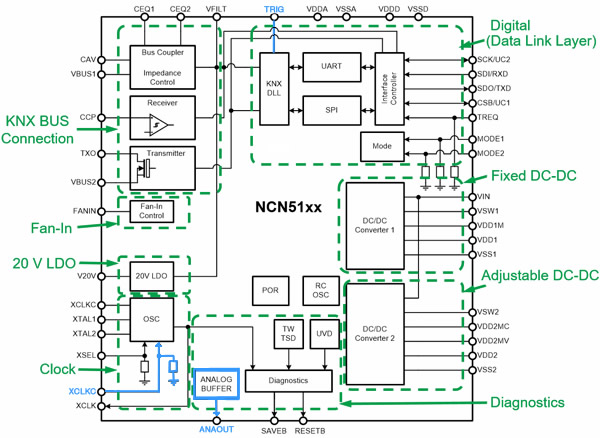
Note: the pins in blue are available for the NCN5121 and NCN5130 only. The NCN5110 does not include the digital block for the data link layer.
The NCN51xx family of transceivers can be used for KNX twisted pair networks (TP1-256). With two DC-DC converters providing a 3.3V fixed and 1.2 to 21V variable range, many applications can be powered from the KNX bus. The transceivers integrate a 20V LDO (Low-dropout) regulator, alongside the lowest voltage KNX bus-coupler drop and low bus current consumption for overall system efficiency. A comprehensive clocking system can generate an 8/16MHz clock for an external microcontroller. For safer and more reliable applications, the NXN51xx family provides an extended ambient temperate range of -40°C to +105°C.
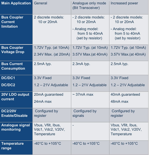
Below is a comparison table showing the different features of ON Semiconductor’s KNX transceiver family. For general needs, the NCN5121 is a popular choice for a number of KNX designers, while the NCN5130 can handle a bus current up to 40mA for higher-power applications. This increased current capability enables multiple applications in a single KNX device. Both transceiver ICs support data link layer communication where UART or SPI is available. The NCN5110 can operate only in analogue mode (PHY), which requires a microcontroller that manages KNX signals coming from, and going through, the twisted pair cable.
Conclusion
By choosing a KNX transceiver from ON Semiconductor, KNX designs are now easier and faster than ever before. It is also possible to diversify the design for different uses and applications simply because all three transceivers are provided in the same package. Drop-in replacement is possible by simply adjusting the value of a couple of external components.
Shawn Back is the Product Marketing Engineer for the Industrial and Offline Products Division of ON Semiconductor, based in Bucheon, Korea. ON Semiconductor is a leading supplier of semiconductor-based solutions, offering a comprehensive portfolio of energy-efficient connectivity, sensing, power management, analogue, logic, timing, discrete, and custom devices. ON Semiconductor has a network of manufacturing facilities, sales offices and design centres in key markets throughout North America, Europe, and the Asia Pacific regions.
